Carbon nanotube
|
|||||||
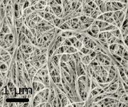
Carbon nanotubes (CNTs; also known as buckytubes) are allotropes of carbon with a cylindrical nanostructure. Nanotubes have been constructed with length-to-diameter ratio of up to 132,000,000:1,[1] which is significantly larger than any other material. These cylindrical carbon molecules have novel properties that make them potentially useful in many applications in nanotechnology, electronics, optics, and other fields of materials science, as well as potential uses in architectural fields. They exhibit extraordinary strength and unique electrical properties, and are efficient thermal conductors.
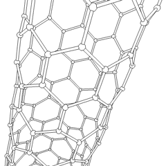
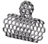
Nanotubes are members of the fullerene structural family, which also includes the spherical buckyballs. The ends of a nanotube might be capped with a hemisphere of the buckyball structure. Their name is derived from their size, since the diameter of a nanotube is on the order of a few nanometers (approximately 1/50,000th of the width of a human hair), while they can be up to 18 centimeters in length (as of 2010).[1] Nanotubes are categorized as single-walled nanotubes (SWNTs) and multi-walled nanotubes (MWNTs).
The nature of the bonding of a nanotube is described by applied quantum chemistry, specifically, orbital hybridization. The chemical bonding of nanotubes is composed entirely of sp2 bonds, similar to those of graphite. This bonding structure, which is stronger than the sp3 bonds found in diamonds, provides the molecules with their unique strength. Nanotubes naturally align themselves into "ropes" held together by Van der Waals forces.
Contents |
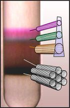
Single-walled
 Armchair (n,n) |
 The chiral vector is bent, while the translation vector stays straight |
 Graphene nanoribbon |
 The chiral vector is bent, while the translation vector stays straight |
 Zigzag (n,0) |
 Chiral (n,m) |
 n and m can be counted at the end of the tube |
 Graphene nanoribbon |
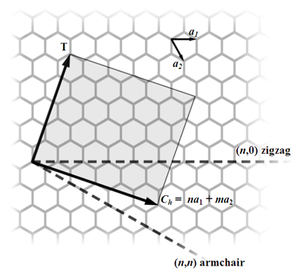

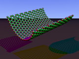
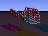
Most single-walled nanotubes (SWNT) have a diameter of close to 1 nanometer, with a tube length that can be many millions of times longer. The structure of a SWNT can be conceptualized by wrapping a one-atom-thick layer of graphite called graphene into a seamless cylinder. The way the graphene sheet is wrapped is represented by a pair of indices (n,m) called the chiral vector. The integers n and m denote the number of unit vectors along two directions in the honeycomb crystal lattice of graphene. If m = 0, the nanotubes are called "zigzag". If n = m, the nanotubes are called "armchair". Otherwise, they are called "chiral". The diameter of a nanotube can be calculated from its (n,m) indices as follows
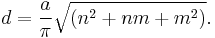
where a = 0.246 nm.
Single-walled nanotubes are an important variety of carbon nanotube because they exhibit electric properties that are not shared by the multi-walled carbon nanotube (MWNT) variants. In particular, their band gap can vary from zero to about 2 eV and their electrical conductivity can show metallic or semiconducting behavior, whereas MWNTs are zero-gap metals. Single-walled nanotubes are the most likely candidate for miniaturizing electronics beyond the micro electromechanical scale currently used in electronics. The most basic building block of these systems is the electric wire, and SWNTs can be excellent conductors.[2][3] One useful application of SWNTs is in the development of the first intramolecular field effect transistors (FET). Production of the first intramolecular logic gate using SWNT FETs has recently become possible as well.[4] To create a logic gate you must have both a p-FET and an n-FET. Because SWNTs are p-FETs when exposed to oxygen and n-FETs otherwise, it is possible to protect half of an SWNT from oxygen exposure, while exposing the other half to oxygen. This results in a single SWNT that acts as a NOT logic gate with both p and n-type FETs within the same molecule.
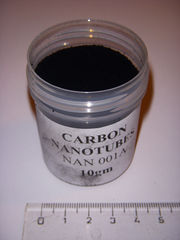
Single-walled nanotubes are dropping precipitously in price, from around $1500 per gram as of 2000 to retail prices of around $50 per gram of as-produced 40–60% by weight SWNTs as of March 2010.[5][6]
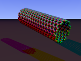
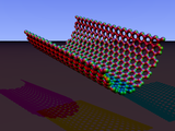
Multi-walled
Multi-walled nanotubes (MWNT) consist of multiple rolled layers (concentric tubes) of graphite. There are two models which can be used to describe the structures of multi-walled nanotubes. In the Russian Doll model, sheets of graphite are arranged in concentric cylinders, e.g. a (0,8) single-walled nanotube (SWNT) within a larger (0,17) single-walled nanotube. In the Parchment model, a single sheet of graphite is rolled in around itself, resembling a scroll of parchment or a rolled newspaper. The interlayer distance in multi-walled nanotubes is close to the distance between graphene layers in graphite, approximately 3.4 Å.
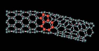
The special place of double-walled carbon nanotubes (DWNT) must be emphasized here because their morphology and properties are similar to SWNT but their resistance to chemicals is significantly improved. This is especially important when functionalization is required (this means grafting of chemical functions at the surface of the nanotubes) to add new properties to the CNT. In the case of SWNT, covalent functionalization will break some C=C double bonds, leaving "holes" in the structure on the nanotube and thus modifying both its mechanical and electrical properties. In the case of DWNT, only the outer wall is modified. DWNT synthesis on the gram-scale was first proposed in 2003[7] by the CCVD technique, from the selective reduction of oxide solutions in methane and hydrogen.
Torus
A nanotorus is theoretically described as carbon nanotube bent into a torus (doughnut shape). Nanotori are predicted to have many unique properties, such as magnetic moments 1000 times larger than previously expected for certain specific radii.[8] Properties such as magnetic moment, thermal stability, etc. vary widely depending on radius of the torus and radius of the tube.[8][9]
Nanobud
Carbon nanobuds are a newly created material combining two previously discovered allotropes of carbon: carbon nanotubes and fullerenes. In this new material, fullerene-like "buds" are covalently bonded to the outer sidewalls of the underlying carbon nanotube. This hybrid material has useful properties of both fullerenes and carbon nanotubes. In particular, they have been found to be exceptionally good field emitters. In composite materials, the attached fullerene molecules may function as molecular anchors preventing slipping of the nanotubes, thus improving the composite’s mechanical properties.
Cup stacked carbon nanotubes
Cup-stacked carbon nanotubes (CSCNTs) differ from other quasi-1D carbon structures that normally behave as a metallic conductor of electrons. CSCNTs exhibit semiconducting behaviors due to the stacking microstructure of graphene layers.[10].
Extreme carbon nanotubes
The observation of the longest carbon nanotubes (18.5 cm long) was reported in 2009. They were grown on Si substrates using an improved chemical vapor deposition (CVD) method and represent electrically uniform arrays of single-walled carbon nanotubes.[1]
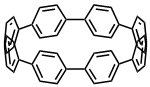
The shortest carbon nanotube is the organic compound cycloparaphenylene which was synthesized in early 2009.[11][12][13]
The thinnest carbon nanotube is armchair (2,2) CNT with a diameter of 3 Å. This nanotube was grown inside a multi-walled carbon nanotube. Assigning of carbon nanotube type was done by combination of high-resolution transmission electron microscopy (HRTEM), Raman spectroscopy and density functional theory (DFT) calculations.[14]
The thinnest freestanding single-walled carbon nanotube is about 4.3 Å in diameter. Researchers suggested that it can be either (5,1) or (4,2) SWCNT, but exact type of carbon nanotube remains questionable.[15] (3,3), (4,3) and (5,1) carbon nanotubes (all about 4 Å in diameter) were unambiguously identified using more precise aberration-corrected high-resolution transmission electron microscopy. However, they were found inside of double-walled carbon nanotubes.[16]
Properties
Strength
Carbon nanotubes are the strongest and stiffest materials yet discovered in terms of tensile strength and elastic modulus respectively. This strength results from the covalent sp² bonds formed between the individual carbon atoms. In 2000, a multi-walled carbon nanotube was tested to have a tensile strength of 63 gigapascals (GPa)[17]. (This, for illustration, translates into the ability to endure tension of a weight equivalent to 6422 kg on a cable with cross-section of 1 mm2.) Since carbon nanotubes have a low density for a solid of 1.3 to 1.4 g·cm−3,[18] its specific strength of up to 48,000 kN·m·kg−1 is the best of known materials, compared to high-carbon steel's 154 kN·m·kg−1.
Under excessive tensile strain, the tubes will undergo plastic deformation, which means the deformation is permanent. This deformation begins at strains of approximately 5% and can increase the maximum strain the tubes undergo before fracture by releasing strain energy.
CNTs are not nearly as strong under compression. Because of their hollow structure and high aspect ratio, they tend to undergo buckling when placed under compressive, torsional or bending stress.[19]
| Material | Young's modulus (TPa) | Tensile strength (GPa) | Elongation at break (%) |
|---|---|---|---|
| SWNT | ~1 (from 1 to 5) | 13–53E | 16 |
| Armchair SWNT | 0.94T | 126.2T | 23.1 |
| Zigzag SWNT | 0.94T | 94.5T | 15.6–17.5 |
| Chiral SWNT | 0.92 | ||
| MWNT | 0.27E[17]–0.8E[24]–0.95E[17] | 11E[17]–63E[17]–150E[24] | |
| Stainless steel | 0.186E[25]–0.214E[26] | 0.38E[25]–1.55E[26] | 15–50 |
| Kevlar–29&149 | 0.06E[27]–0.18E[27] | 3.6E[27]–3.8E[27] | ~2 |
EExperimental observation; TTheoretical prediction
The above discussion referred to axial properties of the nanotube, whereas simple geometrical considerations suggest that carbon nanotubes should be much softer in the radial direction than along the tube axis. Indeed, TEM observation of radial elasticity suggested that even the van der Waals forces can deform two adjacent nanotubes[28]. Nanoindentation experiments, performed by several groups on multiwalled carbon nanotubes,[29][30] indicated Young's modulus of the order of several GPa confirming that CNTs are indeed rather soft in the radial direction.
Hardness
Diamond is considered to be the hardest material, and it is well known that graphite transforms into diamond under conditions of high temperature and high pressure. One study succeeded in the synthesis of a super-hard material by compressing SWNTs to above 24 GPa at room temperature. The hardness of this material was measured with a nanoindenter as 62–152 GPa. The hardness of reference diamond and boron nitride samples was 150 and 62 GPa, respectively. The bulk modulus of compressed SWNTs was 462–546 GPa, surpassing the value of 420 GPa for diamond.[31]
Kinetic
Multi-walled nanotubes, multiple concentric nanotubes precisely nested within one another, exhibit a striking telescoping property whereby an inner nanotube core may slide, almost without friction, within its outer nanotube shell thus creating an atomically perfect linear or rotational bearing. This is one of the first true examples of molecular nanotechnology, the precise positioning of atoms to create useful machines. Already this property has been utilized to create the world's smallest rotational motor[32]. Future applications such as a gigahertz mechanical oscillator are also envisaged.
Electrical

Because of the symmetry and unique electronic structure of graphene, the structure of a nanotube strongly affects its electrical properties. For a given (n,m) nanotube, if n = m, the nanotube is metallic; if n − m is a multiple of 3, then the nanotube is semiconducting with a very small band gap, otherwise the nanotube is a moderate semiconductor. Thus all armchair (n = m) nanotubes are metallic, and nanotubes (6,4), (9,1), etc. are semiconducting.[33]
However, this rule has exceptions, because curvature effects in small diameter carbon nanotubes can influence strongly electrical properties. Thus, (5,0) SWCNT that should be semiconducting is in fact metallic according to the calculations. And vice versa, zigzag and chiral SWCNTs with small diameters that should be metallic have finite gap (armchair nanotubes remain metallic).[33] In theory, metallic nanotubes can carry an electrical current density of 4 × 10⁹ A/cm2 which is more than 1,000 times greater than metals such as copper[34].
Multiwalled carbon nanotubes with interconnected inner shells show superconductivity with a relatively high transition temperature Tc = 12 K. In contrast, the Tc value is an order of magnitude lower for ropes of single-walled carbon nanotubes or for MWNTs with usual, non-interconnected shells.[35]
Optical
Thermal
All nanotubes are expected to be very good thermal conductors along the tube, exhibiting a property known as "ballistic conduction", but good insulators laterally to the tube axis. Measurements show that a SWNT has a room-temperature thermal conductivity along its axis of about 3500 W·m−1·K−1;[36] compare this to copper, a metal well-known for its good thermal conductivity, which transmits 385 W·m−1·K−1. A SWNT has a room-temperature thermal conductivity across its axis of about 1.52 W·m−1·K−1,[37] which is about as thermally conductive as soil. The temperature stability of carbon nanotubes is estimated to be up to 2800 °C in vacuum and about 750 °C in air.[38]
Defects
As with any material, the existence of a crystallographic defect affects the material properties. Defects can occur in the form of atomic vacancies. High levels of such defects can lower the tensile strength by up to 85%. Another form of carbon nanotube defect is the Stone Wales defect, which creates a pentagon and heptagon pair by rearrangement of the bonds. Because of the very small structure of CNTs, the tensile strength of the tube is dependent on its weakest segment in a similar manner to a chain, where the strength of the weakest link becomes the maximum strength of the chain.
Crystallographic defects also affect the tube's electrical properties. A common result is lowered conductivity through the defective region of the tube. A defect in armchair-type tubes (which can conduct electricity) can cause the surrounding region to become semiconducting, and single monoatomic vacancies induce magnetic properties.[39]
Crystallographic defects strongly affect the tube's thermal properties. Such defects lead to phonon scattering, which in turn increases the relaxation rate of the phonons. This reduces the mean free path and reduces the thermal conductivity of nanotube structures. Phonon transport simulations indicate that substitutional defects such as nitrogen or boron will primarily lead to scattering of high-frequency optical phonons. However, larger-scale defects such as Stone Wales defects cause phonon scattering over a wide range of frequencies, leading to a greater reduction in thermal conductivity.[40]
One-dimensional transport
Because of the nanoscale dimensions, electrons propagate only along the tube's axis and electron transport involves many quantum effects. Because of this, carbon nanotubes are frequently referred to as “one-dimensional”.
Toxicity
Determining the toxicity of carbon nanotubes has been one of the most pressing questions in nanotechnology. Unfortunately such research has only just begun and the data are still fragmentary and subject to criticism. Preliminary results highlight the difficulties in evaluating the toxicity of this heterogeneous material. Parameters such as structure, size distribution, surface area, surface chemistry, surface charge, and agglomeration state as well as purity of the samples, have considerable impact on the reactivity of carbon nanotubes. However, available data clearly show that, under some conditions, nanotubes can cross membrane barriers, which suggests that if raw materials reach the organs they can induce harmful effects such as inflammatory and fibrotic reactions.[41]
A study led by Alexandra Porter from the University of Cambridge shows that CNTs can enter human cells and accumulate in the cytoplasm, causing cell death.[42]
Results of rodent studies collectively show that regardless of the process by which CNTs were synthesized and the types and amounts of metals they contained, CNTs were capable of producing inflammation, epithelioid granulomas (microscopic nodules), fibrosis, and biochemical/toxicological changes in the lungs.[43] Comparative toxicity studies in which mice were given equal weights of test materials showed that SWCNTs were more toxic than quartz, which is considered a serious occupational health hazard when chronically inhaled. As a control, ultrafine carbon black was shown to produce minimal lung responses.[44]
The needle-like fiber shape of CNTs, similar to asbestos fibers, raises fears that widespread use of carbon nanotubes may lead to mesothelioma, cancer of the lining of the lungs often caused by exposure to asbestos. A recently-published pilot study supports this prediction.[45] Scientists exposed the mesothelial lining of the body cavity of mice, as a surrogate for the mesothelial lining of the chest cavity, to long multiwalled carbon nanotubes and observed asbestos-like, length-dependent, pathogenic behavior which included inflammation and formation of lesions known as granulomas. Authors of the study conclude:
- "This is of considerable importance, because research and business communities continue to invest heavily in carbon nanotubes for a wide range of products under the assumption that they are no more hazardous than graphite. Our results suggest the need for further research and great caution before introducing such products into the market if long-term harm is to be avoided."[45]
According to co-author Dr. Andrew Maynard:
- "This study is exactly the kind of strategic, highly focused research needed to ensure the safe and responsible development of nanotechnology. It looks at a specific nanoscale material expected to have widespread commercial applications and asks specific questions about a specific health hazard. Even though scientists have been raising concerns about the safety of long, thin carbon nanotubes for over a decade, none of the research needs in the current U.S. federal nanotechnology environment, health and safety risk research strategy address this question."[46]
Although further research is required, results presented today clearly demonstrate that, under certain conditions, especially those involving chronic exposure, carbon nanotubes can pose a serious risk to human health.[41][42][44][45]
Synthesis
Techniques have been developed to produce nanotubes in sizeable quantities, including arc discharge, laser ablation, high pressure carbon monoxide (HiPco), and chemical vapor deposition (CVD). Most of these processes take place in vacuum or with process gases. CVD growth of CNTs can occur in vacuum or at atmospheric pressure. Large quantities of nanotubes can be synthesized by these methods; advances in catalysis and continuous growth processes are making CNTs more commercially viable. A popular commercial process is the CoMoCAT[47], utilized by SouthWest Nanotechnologies.
Arc discharge
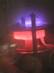
Nanotubes were observed in 1991 in the carbon soot of graphite electrodes during an arc discharge, by using a current of 100 amps, that was intended to produce fullerenes.[48] However the first macroscopic production of carbon nanotubes was made in 1992 by two researchers at NEC's Fundamental Research Laboratory.[49] The method used was the same as in 1991. During this process, the carbon contained in the negative electrode sublimates because of the high discharge temperatures. Because nanotubes were initially discovered using this technique, it has been the most widely-used method of nanotube synthesis.
The yield for this method is up to 30 percent by weight and it produces both single- and multi-walled nanotubes with lengths of up to 50 micrometers with few structural defects.[18]
Laser ablation
In the laser ablation process, a pulsed laser vaporizes a graphite target in a high-temperature reactor while an inert gas is bled into the chamber. Nanotubes develop on the cooler surfaces of the reactor as the vaporized carbon condenses. A water-cooled surface may be included in the system to collect the nanotubes.
This process was developed by Dr. Richard Smalley and co-workers at Rice University, who at the time of the discovery of carbon nanotubes, were blasting metals with a laser to produce various metal molecules. When they heard of the existence of nanotubes they replaced the metals with graphite to create multi-walled carbon nanotubes.[50] Later that year the team used a composite of graphite and metal catalyst particles (the best yield was from a cobalt and nickel mixture) to synthesize single-walled carbon nanotubes.[51]
The laser ablation method yields around 70% and produces primarily single-walled carbon nanotubes with a controllable diameter determined by the reaction temperature. However, it is more expensive than either arc discharge or chemical vapor deposition.[18]
Chemical vapor deposition (CVD)
The catalytic vapor phase deposition of carbon was first reported in 1959,[52] but it was not until 1993[53] that carbon nanotubes were formed by this process. In 2007, researchers at the University of Cincinnati (UC) developed a process to grow aligned carbon nanotube arrays of 18 mm length on a FirstNano ET3000 carbon nanotube growth system.[54]
During CVD, a substrate is prepared with a layer of metal catalyst particles, most commonly nickel, cobalt[55], iron, or a combination[56]. The metal nanoparticles can also be produced by other ways, including reduction of oxides or oxides solid solutions. The diameters of the nanotubes that are to be grown are related to the size of the metal particles. This can be controlled by patterned (or masked) deposition of the metal, annealing, or by plasma etching of a metal layer. The substrate is heated to approximately 700°C. To initiate the growth of nanotubes, two gases are bled into the reactor: a process gas (such as ammonia, nitrogen or hydrogen) and a carbon-containing gas (such as acetylene, ethylene, ethanol or methane). Nanotubes grow at the sites of the metal catalyst; the carbon-containing gas is broken apart at the surface of the catalyst particle, and the carbon is transported to the edges of the particle, where it forms the nanotubes. This mechanism is still being studied. The catalyst particles can stay at the tips of the growing nanotube during the growth process, or remain at the nanotube base, depending on the adhesion between the catalyst particle and the substrate.
CVD is a common method for the commercial production of carbon nanotubes. For this purpose, the metal nanoparticles are mixed with a catalyst support such as MgO or Al2O3 to increase the surface area for higher yield of the catalytic reaction of the carbon feedstock with the metal particles. One issue in this synthesis route is the removal of the catalyst support via an acid treatment, which sometimes could destroy the original structure of the carbon nanotubes. However, alternative catalyst supports that are soluble in water have proven effective for nanotube growth.[57]
If a plasma is generated by the application of a strong electric field during the growth process (plasma enhanced chemical vapor deposition*), then the nanotube growth will follow the direction of the electric field.[58] By adjusting the geometry of the reactor it is possible to synthesize vertically aligned carbon nanotubes[59] (i.e., perpendicular to the substrate), a morphology that has been of interest to researchers interested in the electron emission from nanotubes. Without the plasma, the resulting nanotubes are often randomly oriented. Under certain reaction conditions, even in the absence of a plasma, closely spaced nanotubes will maintain a vertical growth direction resulting in a dense array of tubes resembling a carpet or forest.
Of the various means for nanotube synthesis, CVD shows the most promise for industrial-scale deposition, because of its price/unit ratio, and because CVD is capable of growing nanotubes directly on a desired substrate, whereas the nanotubes must be collected in the other growth techniques. The growth sites are controllable by careful deposition of the catalyst. In 2007, a team from Meijo University demonstrated a high-efficiency CVD technique for growing carbon nanotubes from camphor.[60] Researchers at Rice University, until recently led by the late Richard Smalley, have concentrated upon finding methods to produce large, pure amounts of particular types of nanotubes. Their approach grows long fibers from many small seeds cut from a single nanotube; all of the resulting fibers were found to be of the same diameter as the original nanotube and are expected to be of the same type as the original nanotube.[61]
Super-growth CVD
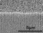
Super-growth CVD (water-assisted chemical vapour deposition) process was developed by Kenji Hata, Sumio Iijima and co-workers at AIST, Japan.[62] In this process, the activity and lifetime of the catalyst are enhanced by addition of water into the CVD reactor. Dense millimeter-tall nanotube "forests", aligned normal to the substrate, were produced. The forests growth rate could be expressed, as

In this equation, β is the initial growth rate and  is the characteristic catalyst lifetime.[63]
Their specific surface exceeds 1,000 m2/g (capped) or 2,200 m2/g (uncapped),[64] surpassing the value of 400–1,000 m2/g for HiPco samples. The synthesis efficiency is about 100 times higher than for the laser ablation method. The time required to make SWNT forests of the height of 2.5 mm by this method was 10 minutes in 2004. Those SWNT forests can be easily separated from the catalyst, yielding clean SWNT material (purity >99.98%) without further purification. For comparison, the as-grown HiPco CNTs contain about 5-35%[65] of metal impurities; it is therefore purified through dispersion and centrifugation that damages the nanotubes. The super-growth process allows to avoid this problem. Patterned highly organized single-walled nanotube structures were successfully fabricated using the super-growth technique.
The mass density of super-growth CNTs is about 0.037 g/cm3.[66][67] It is much lower than that of conventional CNT powders (~1.34 g/cm3), probably because the latter contain metals and amorphous carbon.
The super-growth method is basically a variation of CVD. Therefore, it is possible to grow material containing SWNT, DWNTs and MWNTs, and to alter their ratios by tuning the growth conditions.[68] Their ratios change by the thinness of the catalyst. Many MWNTs are included so that the diameter of the tube is wide.[67]
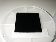
The vertically aligned nanotube forests originate from a "zipping effect" when they are immersed in a solvent and dried. The zipping effect is caused by the surface tension of the solvent and the van der Waals forces between the carbon nanotubes. It aligns the nanotubes into a dense material, which can be formed in various shapes, such as sheets and bars, by applying weak compression during the process. Densification increases the Vickers hardness by about 70 times and density is 0.55 g/cm3. The packed carbon nanotubes are more than 1 mm long and have a carbon purity of 99.9% or higher; they also retain the desirable alignment properties of the nanotubes forest.[69]
Natural, incidental, and controlled flame environments
Fullerenes and carbon nanotubes are not necessarily products of high-tech laboratories; they are commonly formed in such mundane places as ordinary flames,[70] produced by burning methane,[71] ethylene,[72] and benzene,[73] and they have been found in soot from both indoor and outdoor air.[74] However, these naturally occurring varieties can be highly irregular in size and quality because the environment in which they are produced is often highly uncontrolled. Thus, although they can be used in some applications, they can lack in the high degree of uniformity necessary to satisfy the many needs of both research and industry. Recent efforts have focused on producing more uniform carbon nanotubes in controlled flame environments.[75][76][77][78] Such methods have promise for large-scale, low-cost nanotube synthesis, though they must compete with rapidly developing large scale CVD production.
Many electronic applications of carbon nanotubes crucially rely on techniques of selectively producing either semiconducting or metallic CNTs, preferably of a certain chirality. Several methods of separating semiconducting and metallic CNTs are known, but most of them are not yet suitable for large-scale technological processes. The most efficient method relies on density-gradient ultracentrifugation which separates surfactant-wrapped nanotubes by the minute difference in their density. This density difference often translates into difference in the nanotube diameter and (semi)conducting properties.[79] Another method of separation uses a sequence of freezing, thawing, and compression of SWNTs embedded in agarose gel. This process results in a solution containing 70% metallic SWNTs and leaves a gel containing 95% semiconducting SWNTs. The diluted solutions separated by this method show various colors.[80][81] Moreover, SWNTs can be separated by the column chromatography method. Yield is 95% in semiconductor type SWNT and 90% in metallic type SWNT.[82]
In addition to separation of semiconducting and metallic SWNTs, it is possible to sort SWNTs by length, diameter, and chirality. The highest resolution length sorting, with length variation of <10%, has thus far been achieved by size exclusion chromatography (SEC) of DNA-dispersed carbon nanotubes (DNA-SWNT)[83]. SWNT diameter separation has been achieved by density-gradient ultracentrifugation (DGU)[84] using surfactant-dispersed SWNTs and by ion-exchange chromatography (IEC) for DNA-SWNT[85]. Purification of individual chiralities has also been demonstrated with IEC of DNA-SWNT: specific short DNA oligomers can be used to isolate individual SWNT chiralities. Thus far, 12 chiralities have been isolated at purities ranging from 70% for (8,3) and (9,5) SWNTs to 90% for (6,5), (7,5) and (10,5)SWNTs[86]. There have been successful efforts to integrate these purified nanotubes into devices, e. g. FETs [87].
An alternative to separation is development of a selective growth of semiconducting or metallic CNTs. Recently, a new CVD recipe was announced which involves a combination of ethanol and methanol gases and quartz substrates resulting in horizontally aligned arrays of 95–98% semiconducting nanotubes.[88]
Nanotubes are usually grown on nanoparticles of magnetic metal (Fe, Co), which facilitates production of electronic (spintronic) devices. In particular control of current through a field-effect transistor by magnetic field has been demonstrated in such a single-tube nanostructure.[89]
Potential applications
- See also, for last current applications: Timeline of carbon nanotubes
The strength and flexibility of carbon nanotubes makes them of potential use in controlling other nanoscale structures, which suggests they will have an important role in nanotechnology engineering. The highest tensile strength of an individual multi-walled carbon nanotube has been tested to be is 63 GPa.[17] Carbon nanotubes were found in Damascus steel from the 17th century, possibly helping to account for the legendary strength of the swords made of it.[90][91]
Structural
Because of the carbon nanotube's superior mechanical properties, many structures have been proposed ranging from everyday items like clothes and sports gear to combat jackets and space elevators.[92] However, the space elevator will require further efforts in refining carbon nanotube technology, as the practical tensile strength of carbon nanotubes can still be greatly improved.[18]
For perspective, outstanding breakthroughs have already been made. Pioneering work led by Ray H. Baughman at the NanoTech Institute has shown that single and multi-walled nanotubes can produce materials with toughness unmatched in the man-made and natural worlds.[93][94]
In electrical circuits
Nanotube based transistors have been made that operate at room temperature and that are capable of digital switching using a single electron.[95] However, one major obstacle to realization of nanotubes has been the lack of technology for mass production. In 2001 IBM researchers demonstrated how metallic nanotubes can be destroyed, leaving semiconducting ones behind for use as transistors. Their process is called "constructive destruction" which includes the automatic destruction of defective nanotubes on the wafer.[96] This process, however, only gives control over the electrical properties on a statistical scale.
The potential of carbon nanotubes was demonstrated in 2003 when room-temperature ballistic transistors with ohmic metal contacts and high-k gate dielectric were reported, showing 20–30x higher ON current than state-of-the-art Si MOSFETs. This presented an important advance in the field as CNT was shown to potentially outperform Si. At the time, a major challenge was ohmic metal contact formation. In this regard, palladium, which is a high work function metal was shown to exhibit Schottky barrier-free contacts to semiconducting nanotubes with diameters >1.7 nm.[97][98]
The first nanotube integrated memory circuit was made in 2004. One of the main challenges has been regulating the conductivity of nanotubes. Depending on subtle surface features a nanotube may act as a plain conductor or as a semiconductor. A fully automated method has however been developed to remove non-semiconductor tubes.[99]
Another way to make carbon nanotube transistors has been to use random networks of them. By doing so one averages all of their electrical differences and one can produce devices in large scale at the wafer level.[100] This approach was first patented by Nanomix Inc.[101](date of original application June 2002[102] ). It was first published in the academic literature by the United States Naval Research Laboratory in 2003 through independent research work. This approach also enabled Nanomix to make the first transistor on a flexible and transparent substrate.[103][104]
Large structures of carbon nanotubes can be used for thermal management of electronic circuits. An approximately 1 mm–thick carbon nanotube layer was used as a special material to fabricate coolers, this materials has very low density, ~20 times lower weight than a similar copper structure, while the cooling properties are similar for the two materials.[105]
Overall, incorporating carbon nanotubes as transistors into logic-gate circuits with densities comparable to modern CMOS technology has not yet been demonstrated.
As paper batteries
A paper battery is a battery engineered to use a paper-thin sheet of cellulose (which is the major constituent of regular paper, among other things) infused with aligned carbon nanotubes.[106] The nanotubes act as electrodes; allowing the storage devices to conduct electricity. The battery, which functions as both a lithium-ion battery and a supercapacitor, can provide a long, steady power output comparable to a conventional battery, as well as a supercapacitor’s quick burst of high energy—and while a conventional battery contains a number of separate components, the paper battery integrates all of the battery components in a single structure, making it more energy efficient.
Current applications
Current use and application of nanotubes has mostly been limited to the use of bulk nanotubes, which is a mass of rather unorganized fragments of nanotubes. Bulk nanotube materials may never achieve a tensile strength similar to that of individual tubes, but such composites may nevertheless yield strengths sufficient for many applications. Bulk carbon nanotubes have already been used as composite fibers in polymers to improve the mechanical, thermal and electrical properties of the bulk product.
Easton-Bell Sports, Inc. have been in partnership with Zyvex, using CNT technology in a number of their bicycle components—including flat and riser handlebars, cranks, forks, seatposts, stems and aero bars.
Solar cells
Solar cells developed at the New Jersey Institute of Technology use a carbon nanotube complex, formed by a mixture of carbon nanotubes and carbon buckyballs (known as fullerenes) to form snake-like structures. Buckyballs trap electrons, although they can't make electrons flow. Add sunlight to excite the polymers, and the buckyballs will grab the electrons. Nanotubes, behaving like copper wires, will then be able to make the electrons or current flow.[107]
Ultracapacitors
MIT Laboratory for Electromagnetic and Electronic Systems uses nanotubes to improve ultracapacitors. The activated charcoal used in conventional ultracapacitors has many small hollow spaces of various size, which create together a large surface to store electric charge. But as charge is quantized into elementary charges, i.e. electrons, and each such elementary charge needs a minimum space, a significant fraction of the electrode surface is not available for storage because the hollow spaces are not compatible with the charge's requirements. With a nanotube electrode the spaces may be tailored to size—few too large or too small—and consequently the capacity should be increased considerably.[108]
Other applications
Carbon nanotubes have been implemented in nanoelectromechanical systems, including mechanical memory elements (NRAM being developed by Nantero Inc.) and nanoscale electric motors (see Nanomotor).
In May 2005, Nanomix Inc placed on the market a hydrogen sensor which integrated carbon nanotubes on a silicon platform. Since then Nanomix has been patenting many such sensor applications such as in the field of carbon dioxide, nitrous oxide, glucose, DNA detection, etc.
Eikos Inc of Franklin, Massachusetts and Unidym Inc. of Silicon Valley, California are developing transparent, electrically conductive films of carbon nanotubes to replace indium tin oxide (ITO). Carbon nanotube films are substantially more mechanically robust than ITO films, making them ideal for high-reliability touchscreens and flexible displays. Printable water-based inks of carbon nanotubes are desired to enable the production of these films to replace ITO.[109] Nanotube films show promise for use in displays for computers, cell phones, PDAs, and ATMs.
A nanoradio, a radio receiver consisting of a single nanotube, was demonstrated in 2007. In 2008 it was shown that a sheet of nanotubes can operate as a loudspeaker if an alternating current is applied. The sound is not produced through vibration but thermoacoustically.[110]
Because of the high mechanical strength of carbon nanotubes, research is being made into weaving them into clothes to create stab-proof and bulletproof clothing. The nanotubes would effectively stop the bullet from penetrating the body, although the bullet's kinetic energy would likely cause broken bones and internal bleeding.[111]
A flywheel made of carbon nanotubes could be spun at extremely high velocity on a floating magnetic axis in a vacuum, and potentially store energy at a density approaching that of conventional fossil fuels. Since energy can be added to and removed from flywheels very efficiently in the form of electricity, this might offer a way of storing electricity, making the electrical grid more efficient and variable power suppliers (like wind turbines) more useful in meeting energy needs. The practicality of this depends heavily upon the cost of making massive, unbroken nanotube structures, and their failure rate under stress. Ultra-short SWNTs (US-tubes) have been used as nanoscaled capsules for delivering MRI contrast agents in vivo. [112]
Nitrogen-doped carbon nanotubes may replace platinum catalysts used to reduce oxygen in fuel cells. A forest of vertically-aligned nanotubes can reduce oxygen in alkaline solution more effectively than platinum, which has been used in such applications since the 1960s. The nanotubes have the added benefit of not being subject to carbon monoxide poisoning.[113]
Discovery
A 2006 editorial written by Marc Monthioux and Vladimir Kuznetsov in the journal Carbon described the interesting and often misstated origin of the carbon nanotube. A large percentage of academic and popular literature attributes the discovery of hollow, nanometer-size tubes composed of graphitic carbon to Sumio Iijima of NEC in 1991.[114]
In 1952 L. V. Radushkevich and V. M. Lukyanovich published clear images of 50 nanometer diameter tubes made of carbon in the Soviet Journal of Physical Chemistry.[115] This discovery was largely unnoticed, as the article was published in the Russian language, and Western scientists' access to Soviet press was limited during the Cold War. It is likely that carbon nanotubes were produced before this date, but the invention of the transmission electron microscope (TEM) allowed direct visualization of these structures.
Carbon nanotubes have been produced and observed under a variety of conditions prior to 1991. A paper by Oberlin, Endo, and Koyama published in 1976 clearly showed hollow carbon fibers with nanometer-scale diameters using a vapor-growth technique.[116] Additionally, the authors show a TEM image of a nanotube consisting of a single wall of graphene. Later, Endo has referred to this image as a single-walled nanotube.[117]
In 1979 John Abrahamson presented evidence of carbon nanotubes at the 14th Biennial Conference of Carbon at Pennsylvania State University. The conference paper described carbon nanotubes as carbon fibers which were produced on carbon anodes during arc discharge. A characterization of these fibers was given as well as hypotheses for their growth in a nitrogen atmosphere at low pressures.[118]
In 1981 a group of Soviet scientists published the results of chemical and structural characterization of carbon nanoparticles produced by a thermocatalytical disproportionation of carbon monoxide. Using TEM images and XRD patterns, the authors suggested that their “carbon multi-layer tubular crystals” were formed by rolling graphene layers into cylinders. They speculated that by rolling graphene layers into a cylinder, many different arrangements of graphene hexagonal nets are possible. They suggested two possibilities of such arrangements: circular arrangement (armchair nanotube) and a spiral, helical arrangement (chiral tube).[119]
In 1987, Howard G. Tennett of Hyperion Catalysis was issued a U.S. patent for the production of "cylindrical discrete carbon fibrils" with a "constant diameter between about 3.5 and about 70 nanometers..., length 102 times the diameter, and an outer region of multiple essentially continuous layers of ordered carbon atoms and a distinct inner core...."[120]
Iijima's discovery of multi-walled carbon nanotubes in the insoluble material of arc-burned graphite rods in 1991[121] and Mintmire, Dunlap, and White's independent prediction that if single-walled carbon nanotubes could be made, then they would exhibit remarkable conducting properties [122] helped create the initial buzz that is now associated with carbon nanotubes. Nanotube research accelerated greatly following the independent discoveries[123][124] by Bethune at IBM[125] and Iijima at NEC of single-walled carbon nanotubes and methods to specifically produce them by adding transition-metal catalysts to the carbon in an arc discharge. The arc discharge technique was well-known to produce the famed Buckminster fullerene on a preparative scale,[126] and these results appeared to extend the run of accidental discoveries relating to fullerenes. The original observation of fullerenes in mass spectrometry was not anticipated,[127] and the first mass-production technique by Krätschmer and Huffman was used for several years before realizing that it produced fullerenes.[126]
The discovery of nanotubes remains a contentious issue. Many believe that Iijima's report in 1991 is of particular importance because it brought carbon nanotubes into the awareness of the scientific community as a whole.[114]
See also
- Allotropes of carbon
- Boron nitride nanotube
- Carbon nanotubes in photovoltaics
- Nanoflower
- Graphene
- Buckypaper
- Graphene oxide paper
- Carbon nanotube chemistry
- List of software for nanostructures modeling
- Optical properties of carbon nanotubes
- Organic electronics
- Selective chemistry of single-walled nanotubes
- Potential applications of carbon nanotubes
- List of Carbon Nanotube Suppliers
- Colossal carbon tube
- Molecular modeling
- Silicon nanotubes
- Tunable nanoporous carbon
- Carbon nanoparticles
- Carbon nanofibers
- Carbon nanocone
Free-download reviews
- NT06 - the major CNT event - click the speakers
- NT05 - click the "HERE"s
- Selection of free-download articles on carbon nanotubes
Books
- Carbon Nanotube Science, by P.J.F. Harris, Cambridge University Press, 2009.
- Book : Carbon Nanotube - Multifunctional Material, Edited by Prakash R. Somani and M. Umeno, Applied Science Innovations Pvt. Ltd., India.
- The Application of Carbon Nanotubes and Graphene to Electronics.
References
- ↑ 1.0 1.1 1.2 Wang, X.; Li, Q.; Xie, J.; Jin, Z.; Wang, J.; Li, Y.; Jiang, K.; Fan, S. (2009). "Fabrication of Ultralong and Electrically Uniform Single-Walled Carbon Nanotubes on Clean Substrates". Nano Letters 9 (9): 3137–3141. doi:10.1021/nl901260b. PMID 19650638.
- ↑ Mintmire, J.W.; Dunlap, BI; White, CT (3 February 1992). "Are Fullerene Tubules Metallic?". Physical Review Letters 68 (5): 631–634. doi:10.1103/PhysRevLett.68.631. PMID 10045950.
- ↑ Dekker, Cees (1999). "Carbon nanotubes as molecular quantum wires" (PDF). Physics Today 52: 22–28. doi:10.1063/1.882658. http://www.physicstoday.org/vol-56/iss-2/pdf/vol52no5p22-28.pdf.
- ↑ Martel, R.; Derycke, V.; Lavoie, C.; Appenzeller, J.; Chan, K. K.; Tersoff, J.; Avouris, Ph. (2001). "Ambipolar Electrical Transport in Semiconducting Single-Wall Carbon Nanotubes". Physical Review Letters 87: 256805. doi:10.1103/PhysRevLett.87.256805.
- ↑ "Carbon Solutions, Inc.". http://www.carbonsolution.com.
- ↑ "CarboLex". http://carbolex.com.
- ↑ Flahaut, E.; Bacsa, R; Peigney, A; Laurent, C (2003). "Gram-Scale CCVD Synthesis of Double-Walled Carbon Nanotubes". Chemical Communications 12 (12): 1442–1443. doi:10.1039/b301514a. PMID 12841282.
- ↑ 8.0 8.1 Liu, Lei; Guo, G. Y.; Jayanthi, C. S.; Wu, S. Y. (2002). "Colossal Paramagnetic Moments in Metallic Carbon Nanotori". Physical Review Letters 88: 217206. doi:10.1103/PhysRevLett.88.217206.
- ↑ Huhtala, Maria (2002). "Carbon nanotube structures: molecular dynamics simulation at realistic limit" (PDF). Computer Physics Communications 146: 30. doi:10.1016/S0010-4655(02)00432-0. http://www.princeton.edu/~msammalk/publications/cpc146_02.pdf.
- ↑ Liu, Q; Ren, W; Chen, Z; Yin, L; Li, F; Cong, H; Cheng, H (2009). "Semiconducting properties of cup-stacked carbon nanotubes". Carbon 47: 731. doi:10.1016/j.carbon.2008.11.005. http://carbon.imr.ac.cn/file/Journal/2009/1249016438117.pdf.
- ↑ "A Better Way to Make Nanotubes". Berkeley Lab.. January 5, 2009. http://newscenter.lbl.gov/feature-stories/2009/01/05/better-way-to-make-nanotubes/.
- ↑ "Carbon Nanohoops: Shortest Segment of a Carbon Nanotube Synthesized". Berkeley Lab.. http://www.lbl.gov/msd/assets/docs/highlights/09-Bertozzi.pdf.
- ↑ "Synthetic organic chemistry". A centre of chemistry excellence. Nature. October 7, 2009. http://www.nature.com/naturejobs/2009/091008/full/nj0264.html#a-centre-of-chemistry-excellence.
- ↑ Zhao, X.; Liu, Y.; Inoue, S.; Suzuki, T.; Jones, R. O.; Andol, Y. (2004). "Smallest Carbon Nanotube is 3 Å in Diameter". Physical Review Letters 92 (12): 125502. doi:10.1103/PhysRevLett.92.125502. PMID 15089683.
- ↑ Hayashi, Takuya; Kim, Yoong Ahm; Matoba, Toshiharu; Esaka, Masaya; Nishimura, Kunio; Tsukada, Takayuki; Endo, Morinobu; Dresselhaus, Mildred S. (2003). "Smallest Freestanding Single-Walled Carbon Nanotube". Nano Letters 3 (7): 887–889. doi:10.1021/nl034080r.
- ↑ Guan, Lunhui; Suenaga, Kazu; Iijima, Sumio (2008). "Smallest Carbon Nanotube Assigned with Atomic Resolution Accuracy". Nano Letters 8 (2): 459–462. doi:10.1021/nl072396j. PMID 18186659.
- ↑ 17.0 17.1 17.2 17.3 17.4 17.5 Yu, Min-Feng; Lourie, Oleg; Dyer, Mark J.; Moloni, Katerina; Kelly, Thomas F.; Ruoff, Rodney S. (28 January 2000). "Strength and Breaking Mechanism of Multiwalled Carbon Nanotubes Under Tensile Load". Science 287 (5453): 637–640. doi:10.1126/science.287.5453.637. PMID 10649994.
- ↑ 18.0 18.1 18.2 18.3 Collins, Philip G. (2000). "Nanotubes for Electronics" (PDF). Scientific American: 67–69. http://www.crhc.uiuc.edu/ece497nc/fall01/papers/NTs_SciAm_2000.pdf.
- ↑ K. Jensen, W. Mickelson, A. Kis, and A. Zettl. Buckling and kinking force measurements on individual multiwalled carbon nanotubes. Phys. Rev. B 76, 195436 (2007)
- ↑ Belluci, S. (19 January 2005). "Carbon nanotubes: physics and applications". Physica Status Solidi (c) 2 (1): 34–47. doi:10.1002/pssc.200460105.
- ↑ Chae, Han Gi; Kumar, Satish (26 January 2006). "Rigid Rod Polymeric Fibers". Journal of Applied Polymer Science 100 (1): 791–802. doi:10.1002/app.22680.
- ↑ Meo, Michele; Rossi, Marco (3 February 2006). "Prediction of Young’s modulus of single wall carbon nanotubes by molecular-mechanics based finite element modelling". Composites Science and Technology 66 (11–12): 1597–1605. doi:10.1016/j.compscitech.2005.11.015.
- ↑ Sinnott, Susan B.; Andrews, Rodney (July 2001). "Carbon Nanotubes: Synthesis, Properties, and Applications". Critical Reviews in Solid State and Materials Sciences 26 (3): 145–249. doi:10.1080/20014091104189.
- ↑ 24.0 24.1 Demczyk, B.G.; Wang, Y.M.; Cumings, J.; Hetman, M.; Han, W.; Zettl, A.; Ritchie, R.O. (13 June 2002). "Direct mechanical measurement of the tensile strength and elastic modulus of multiwalled carbon nanotubes". Materials Science and Engineering A 334 (1–2): 173–178. doi:10.1016/S0921-5093(01)01807-X.
- ↑ 25.0 25.1 Australian Stainless Steel Development Association (ASSDA) - Properties of Stainless Steel
- ↑ 26.0 26.1 Stainless Steel - 17-7PH (Fe/Cr17/Ni 7) Material Information
- ↑ 27.0 27.1 27.2 27.3 H. D. Wagner (2002). "Reinforcement". Encyclopedia of Polymer Science and Technology. John Wiley & Sons. doi:10.1002/0471440264.pst317. http://www.weizmann.ac.il/wagner/COURSES/Reading%20material%20(papers)/Encyclopedy_of_polymer_science_2003.pdf.
- ↑ R. S. Ruoff, et al., "Radial deformation of carbon nanotubes by van der Waals forces" Nature 364, 514 (1993)
- ↑ I. Palaci, et al. "Radial Elasticity of Multiwalled Carbon Nanotubes" Phys. Rev. Lett. 94, 175502 (2005)
- ↑ M.-F. Yu, et al. "Investigation of the Radial Deformability of Individual Carbon Nanotubes under Controlled Indentation Force" Phys. Rev. Lett. 85, 1456-1459 (2000)
- ↑ M. Popov et al. (2002). "Superhard phase composed of single-wall carbon nanotubes" (free download PDF). Phys. Rev. B 65: 033408. doi:10.1103/PhysRevB.65.033408. http://www.ssl.physics.ncsu.edu/publication/browse/getFileAction?fileref=2003-02-27+12:53:01&dbfilename=2002-PRB65-033408.pdf.
- ↑ 07.23.2003 - Physicists build world's smallest motor using nanotubes and etched silicon
- ↑ 33.0 33.1 Lu, X.; Chen, Z. (2005). "Curved Pi-Conjugation, Aromaticity, and the Related Chemistry of Small Fullerenes (<C60) and Single-Walled Carbon Nanotubes". Chemical Reviews 105 (10): 3643–3696. doi:10.1021/cr030093d. PMID 16218563.
- ↑ Hong, Seunghun; Myung, S (2007). "Nanotube Electronics: A flexible approach to mobility". Nature Nanotechnology 2 (4): 207–208. doi:10.1038/nnano.2007.89. PMID 18654263.
- ↑ J. Haruyama et al. (2006). "Superconductivity in Entirely End-Bonded Multiwalled Carbon Nanotubes" (free download PDF). Physical Review Letters 96: 057001. doi:10.1103/PhysRevLett.96.057001. http://www.ee.aoyama.ac.jp/Labs/j-haru-www/paper/Haruyama%20SuperCNT%20PRL%20publication.pdf.
- ↑ Pop, Eric et al.; Mann, David; Wang, Qian; Goodson, Kenneth; Dai, Hongjie (2005-12-22). "Thermal conductance of an individual single-wall carbon nanotube above room temperature". Nano Letters 6 (1): 96–100. doi:10.1021/nl052145f. PMID 16402794.
- ↑ Sinha, Saion et al.; Barjami, Saimir; Iannacchione, Germano; Schwab, Alexander; Muench, George (2005-06-05). "Off-axis thermal properties of carbon nanotube films". Journal of Nanoparticle Research 7 (6): 651–657. doi:10.1007/s11051-005-8382-9.
- ↑ Thostenson, Erik; Li, C; Chou, T (2005). "Nanocomposites in context". Composites Science and Technology 65: 491–516. doi:10.1016/j.compscitech.2004.11.003.
- ↑ Carbon Based Magnetism: An Overview of the Magnetism of Metal Free Carbon-based Compounds and Materials, edited by Tatiana Makarova and Fernando Palacio (Elsevier 2006)
- ↑ Mingo, N.; Stewart, D. A.; Broido, D. A.; Srivastava, D. (2008). "Phonon transmission through defects in carbon nanotubes from first principles". Physical Review B 77: 033418. doi:10.1103/PhysRevB.77.033418.
- ↑ 41.0 41.1 Kolosnjaj J, Szwarc H, Moussa F (2007). "Toxicity studies of carbon nanotubes". Adv Exp Med Biol. 620: 181–204. doi:10.1007/978-0-387-76713-0_14. PMID 18217344.
- ↑ 42.0 42.1 Porter, Alexandra; Gass, Mhairi; Muller, Karin; Skepper, Jeremy N.; Midgley, Paul A.; Welland, Mark (2007). "Direct imaging of single-walled carbon nanotubes in cells". Nature Nanotechnology 2 (11): 713. doi:10.1038/nnano.2007.347. PMID 18654411.
- ↑ Zumwalde, Ralph and Laura Hodson (March 2009). "Approaches to Safe Nanotechnology: Managing the Health and Safety Concerns Associated with Engineered Nanomaterials". National Institute for Occupational Safety and Health. NIOSH (DHHS) Publication 2009-125.
- ↑ 44.0 44.1 Lam CW, James JT, McCluskey R, Arepalli S, Hunter RL (2006). "A review of carbon nanotube toxicity and assessment of potential occupational and environmental health risks". Crit Rev Toxicol. 36 (3): 189–217. doi:10.1080/10408440600570233. PMID 16686422.
- ↑ 45.0 45.1 45.2 Poland, CA; Duffin, Rodger; Kinloch, Ian; Maynard, Andrew; Wallace, William A. H.; Seaton, Anthony; Stone, Vicki; Brown, Simon et al. (2008). "Carbon nanotubes introduced into the abdominal cavity of mice show asbestos-like pathogenicity in a pilot study.". Nature Nanotechnology 3 (7): 423. doi:10.1038/nnano.2008.111. PMID 18654567.
- ↑ Carbon Nanotubes That Look Like Asbestos, Behave Like Asbestos
- ↑ "Method of Producing Carbon Nanotubes" US Patent 6,333,016 (2001)
- ↑ Iijima, Sumio (1991). "Helical microtubules of graphitic carbon". Nature 354: 56–58. doi:10.1038/354056a0.
- ↑ Ebbesen, T. W.; Ajayan, P. M. (1992). "Large-scale synthesis of carbon nanotubes". Nature 358: 220–222. doi:10.1038/358220a0.
- ↑ Guo, Ting; Nikolaev, Pavel; Rinzler, Andrew G.; Tomanek, David; Colbert, Daniel T.; Smalley, Richard E. (1995). "Self-Assembly of Tubular Fullerenes". J. Phys. Chem. 99: 10694–10697. doi:10.1021/j100027a002. http://www.pa.msu.edu/cmp/csc/eprint/DT085.pdf.
- ↑ Guo, Ting; Nikolaev, P; Thess, A; Colbert, D; Smalley, R (1995). "Catalytic growth of single-walled nanotubes by laser vaporization" (PDF). Chem. Phys. Lett. 243: 49–54. doi:10.1016/0009-2614(95)00825-O. http://www.orgchem.science.ru.nl/molmat/mm-web/education/caput-college/ChemPhysLett-1995-243-49.pdf.
- ↑ Walker Jr., P. L.; Rakszawski, J. F.; Imperial, G. R. (1959). "Carbon Formation from Carbon Monoxide-Hydrogen Mixtures over Iron Catalysts. I. Properties of Carbon Formed". J. Phys. Chem. 63: 133. doi:10.1021/j150572a002.
- ↑ José-Yacamán, M.; Miki-Yoshida, M.; Rendón, L.; Santiesteban, J. G. (1993). "Catalytic growth of carbon microtubules with fullerene structure". Appl. Phys. Lett. 62: 657. doi:10.1063/1.108857.
- ↑ Beckman, Wendy (2007-04-27). "UC Researchers Shatter World Records with Length of Carbon Nanotube Arrays". University of Cincinnati. http://www.uc.edu/news/NR.asp?id=5700.
- ↑ N. Inami et al. "Synthesis-condition dependence of carbon nanotube growth by alcohol catalytic chemical vapor deposition method" Sci. Technol. Adv. Mater. 8 (2007) 292 free download
- ↑ N. Ishigami; Ago, H; Imamoto, K; Tsuji, M; Iakoubovskii, K; Minami, N (2008). "Crystal Plane Dependent Growth of Aligned Single-Walled Carbon Nanotubes on Sapphire". J. Am. Chem. Soc. 130 (30): 9918–9924. doi:10.1021/ja8024752. PMID 18597459.
- ↑ Eftekhari, A.; Jafarkhani, P; Moztarzadeh, F (2006). "High-yield synthesis of carbon nanotubes using a water-soluble catalyst support in catalytic chemical vapor deposition". Carbon 44: 1343. doi:10.1016/j.carbon.2005.12.006.
- ↑ Ren, Z. F.; Huang, ZP; Xu, JW; Wang, JH; Bush, P; Siegal, MP; Provencio, PN (1998). "Synthesis of Large Arrays of Well-Aligned Carbon Nanotubes on Glass". Science 282 (5391): 1105. doi:10.1126/science.282.5391.1105. PMID 9804545.
- ↑ SEM images & TEM images of carbon nanotubes, aligned carbon nanotube arrays, and nanoparticles
- ↑ "Carbon Nanotubes from Camphor: An Environment-Friendly Nanotechnology" (free download PDF). Journal of Physics: Conference Series 61: 643. 2007. http://www.iop.org/EJ/article/1742-6596/61/1/129/jpconf7_61_129.pdf.
- ↑ Boyd, Jade (2006-11-17). "Rice chemists create, grow nanotube seeds". Rice University. http://www.media.rice.edu/media/NewsBot.asp?MODE=VIEW&ID=9070.
- ↑ K. Hata et al. (2004). "Water-Assisted Highly Efficient Synthesis of Impurity-Free Single-Walled Carbon Nanotubes". Science 306 (5700): 1362–1365. doi:10.1126/science.1104962. PMID 15550668.
- ↑ K. Hata et al. (2005). "Kinetics of Water-Assisted Single-Walled Carbon Nanotube Synthesis Revealed by a Time-Evolution Analysis". Physical Review Letters 95: 056104. doi:10.1103/PhysRevLett.95.056104.
- ↑ K. Hata, Sumio Iijima et al. (2009). "Compact and light supercapacitors from a surface-only solid by opened carbon nanotubes with 2,200 m2/g". Advanced Functional Materials 20: 422–428. doi:10.1002/adfm.200901927.
- ↑ "Unidym product sheet SWNT" (free download PDF). http://www.unidym.com/files/Unidym_Product_Sheet_SWNT.pdf.
- ↑ "Characteristic of Carbon nanotubes by super-growth method" (in japanese). http://www.nanocarbon.jp/sg/002.html.
- ↑ 67.0 67.1 K.Hata. "From Highly Efficient Impurity-Free CNT Synthesis to DWNT forests, CNTsolids and Super-Capacitors" (free download PDF). http://www.nanocarbon.jp/english/research/image/review.pdf.
- ↑ Takeo Yamada et al. (2006). "Size-selective growth of double-walled carbon nanotube forests from engineered iron catalysts". Nature Nanotechnology 1 (2): 131–136. doi:10.1038/nnano.2006.95. PMID 18654165.
- ↑ Don N. Futaba , Kenji Hata et al. (2006). "Shape-engineerable and highly densely packed single-walled carbon nanotubes and their application as super-capacitor electrodes". Nature Materials 5 (12): 987–994. doi:10.1038/nmat1782. PMID 17128258.
- ↑ Singer, J.M. (1959). "Carbon formation in very rich hydrocarbon-air flames. I. Studies of chemical content, temperature, ionization and particulate matter". Seventh Symposium (International) on Combustion.
- ↑ Yuan, Liming (2001). "Nanotubes from methane flames". Chemical physics letters 340: 237–241. doi:10.1016/S0009-2614(01)00435-3.
- ↑ Yuan, Liming (2001). "Ethylene flame synthesis of well-aligned multi-walled carbon nanotubes". Chemical physics letters 346: 23–28. doi:10.1016/S0009-2614(01)00959-9.
- ↑ Duan, H. M.; McKinnon, J. T. (1994). "Nanoclusters Produced in Flames". Journal of Physical Chemistry 98: 12815–12818. doi:10.1021/j100100a001.
- ↑ Murr, L. E.; Bang, J.J.; Esquivel, E.V.; Guerrero, P.A.; Lopez, D.A. (2004). "Carbon nanotubes, nanocrystal forms, and complex nanoparticle aggregates in common fuel-gas combustion sources and the ambient air". Journal of Nanoparticle Research 6: 241–251. doi:10.1023/B:NANO.0000034651.91325.40.
- ↑ Vander Wal, R.L. (2002). "Fe-catalyzed single-walled carbon nanotube synthesis within a flame environment". Combust. Flame 130: 37–47. doi:10.1016/S0010-2180(02)00360-7.
- ↑ Saveliev, A.V. (2003). "Metal catalyzed synthesis of carbon nanostructures in an opposed flow methane oxygen flame". Combust. Flame 135: 27–33. doi:10.1016/S0010-2180(03)00142-1.
- ↑ Height, M.J. (2004). "Flame synthesis of single-walled carbon nanotubes". Carbon 42: 2295–2307. doi:10.1016/j.carbon.2004.05.010.
- ↑ Sen, S.; Puri, Ishwar K (2004). "Flame synthesis of carbon nanofibers and nanofibers composites containing encapsulated metal particles". Nanotechnology 15: 264–268. doi:10.1088/0957-4484/15/3/005.
- ↑ 79.0 79.1 Arnold, Michael S.; Green, Alexander A.; Hulvat, James F.; Stupp, Samuel I.; Hersam, Mark C. (2006). "Sorting carbon nanotubes by electronic structure using density differentiation". Nature Nanotechnology 1 (1): 60. doi:10.1038/nnano.2006.52. PMID 18654143.
- ↑ Takeshi Tanaka et al. (2009). "Simple and Scalable Gel-Based Separation of Metallic and Semiconducting Carbon Nanotubes". Nano Letters 9 (4): 1497–1500. doi:10.1021/nl8034866. PMID 19243112.
- ↑ T.Tanaka. "New, Simple Method for Separation of Metallic and Semiconducting Carbon Nanotubes". http://www.aist.go.jp/aist_e/latest_research/2009/20090406/20090406.html.
- ↑ Takeshi Tanaka et al. (2009). "Continuous Separation of Metallic and Semiconducting Carbon Nanotubes Using Agarose Gel". Applied Physics Express 2: 125002. doi:10.1143/APEX.2.125002.
- ↑ Huang, X et al. (2005). "High-Resolution Length Sorting and Purification of DNA-Wrapped Carbon Nanotubes by Size-Exclusion Chromatography". Anal. Chem. 77 (19): 6225–6228. doi:10.1021/ac0508954. PMID 16194082.
- ↑ Mark C Hersam (2008). "Progress towards monodisperse single-walled carbon nanotubes". Nature Nanotechnology 3 (7): 387–394. doi:10.1038/nnano.2008.135. PMID 18654561.
- ↑ Zheng, M et al. (2003). "Structure-Based Carbon Nanotube Sorting by Sequence-Dependent DNA Assembly". Science 302 (5650): 1545–1548. doi:10.1126/science.1091911. PMID 14645843.
- ↑ Tu, Helen et al. (2009). "DNA sequence motifs for structure-specific recognition and separation of carbon nanotubes". Nature 460 (7252): 250–253. doi:10.1038/nature08116. PMID 19587767.
- ↑ Zhang, L et al. (2009). "Optical characterizations and electronic devices of nearly pure (10,5) single-walled carbon nanotubes.". J Am Chem Soc 131 (7): 2454–2455. doi:10.1021/ja8096674. PMID 19193007.
- ↑ Ding, Lei; Tselev, Alexander; Wang, Jinyong; Yuan, Dongning; Chu, Haibin; McNicholas, Thomas P.; Li, Yan; Liu, Jie (2009). "Selective Growth of Well-Aligned Semiconducting Single-Walled Carbon Nanotubes". Nano Letters 9 (2): 800. doi:10.1021/nl803496s. PMID 19159186.
- ↑ M.A. Mohamed; Ambri Mohamed, Mohd; Shikoh, Eiji; Fujiwara, Akihiko (2007). "Fabrication of spintronics device by direct synthesis of single-walled carbon nanotubes from ferromagnetic electrodes" (free download pdf). Sci. Technol. Adv. Mater. 8: 292. doi:10.1016/j.stam.2007.02.009.
- ↑ K. Sanderson (2006). "Sharpest cut from nanotube sword". Nature 444: 286. doi:10.1038/news061113-11.
- ↑ Reibold, M.; Paufler, P; Levin, AA; Kochmann, W; Pätzke, N; Meyer, DC (November 16, 2006). "Materials:Carbon nanotubes in an ancient Damascus sabre". Nature 444 (7117): 286. doi:10.1038/444286a. PMID 17108950.
- ↑ Edwards, Brad C. (2003). The Space Elevator. BC Edwards. ISBN 0974651710.
- ↑ Zhang, Mei; Fang, S; Zakhidov, AA; Lee, SB; Aliev, AE; Williams, CD; Atkinson, KR; Baughman, RH (2005). "Strong, Transparent, Multifunctional, Carbon Nanotube Sheets". Science 309 (5738): 1215–1219. doi:10.1126/science.1115311. PMID 16109875.
- ↑ Dalton, Alan B.; Su, Tian; Horng, Tiffany; Chow, Amy; Akira, Shizuo; Medzhitov, Ruslan (2003). "Super-tough carbon-nanotube fibres". Nature 423 (4): 703. doi:10.1038/ni1569. PMID 18297073.
- ↑ Postma, Henk W. Ch.; Teepen, T; Yao, Z; Grifoni, M; Dekker, C (2001). "Carbon Nanotube Single-Electron Transistors at Room temperature". Science 293 (5527): 76. doi:10.1126/science.1061797. PMID 11441175.
- ↑ Collins, Philip G.; Arnold, MS; Avouris, P (2001). "Engineering Carbon Nanotubes and Nanotube Circuits Using Electrical Breakdown". Science 292 (5517): 706–709. doi:10.1126/science.1058782. PMID 11326094.
- ↑ Javey, Ali; Guo, J; Wang, Q; Lundstrom, M; Dai, H (2003). "Ballistic Carbon Nanotube Transistors". Nature 424 (6949): 654–657. doi:10.1038/nature01797. PMID 12904787.
- ↑ Javey, Ali; Guo, J; Farmer, D; Wang, Q; Yenilmez, E; Gordon, R; Lundstrom, M; Dai, H (2004). "Self-aligned ballistic molecular transistors and electrically parallel nanotube arrays". Nano Letters 4: 1319–1322. doi:10.1021/nl049222b.
- ↑ Tseng, Yu-Chih; Xuan, Peiqi; Javey, Ali; Malloy, Ryan; Wang, Qian; Bokor, Jeffrey; Dai, Hongjie (2004). "Monolithic Integration of Carbon Nanotube Devices with Silicon MOS Technology". Nano Letters 4: 123–127. doi:10.1021/nl0349707.
- ↑ Gabriel, Jean-Christophe P. (2003). "Large Scale Production of Carbon Nanotube Transistors: A Generic Platforms for Chemical Sensors". Mat. Res. Soc. Symp. Proc. 762: Q.12.7.1. http://www.mrs.org/s_mrs/sec_subscribe.asp?CID=2606&DID=110422&action=detail.
- ↑ Nanōmix - Breakthrough Detection Solutions with the Nanoelectronic Sensation Technology
- ↑ Gabriel, Jean-Christophe P.. "Dispersed Growth Of Nanotubes on a substrate". Patent WO 2004040671A2. http://www.freepatentsonline.com/EP1560958.html.
- ↑ Bradley, Keith; Gabriel, Jean-Christophe P.; Grüner, George (2003). "Flexible nanotube transistors". Nano Letters 3: 1353–1355. doi:10.1021/nl0344864.
- ↑ Armitage, Peter N.. "Flexible nanostructure electronic devices". United States Patent 20050184641 A1. http://www.freshpatents.com/Flexible-nanostructure-electronic-devices-dt20050825ptan20050184641.php.
- ↑ K. Kordas; Tóth, G.; Moilanen, P.; Kumpumäki, M.; Vähäkangas, J.; Uusimäki, A.; Vajtai, R.; Ajayan, P. M. (2007). "Chip cooling with integrated carbon nanotube microfin architectures". Appl. Phys. Lett. 90: 123105. doi:10.1063/1.2714281.
- ↑ "Beyond Batteries: Storing Power in a Sheet of Paper". Eurekalert.org. August 13, 2007. http://www.eurekalert.org/pub_releases/2007-08/rpi-bbs080907.php. Retrieved 2008-09-15.
- ↑ "New Flexible Plastic Solar Panels Are Inexpensive And Easy To Make". ScienceDaily. July 19, 2007. http://www.sciencedaily.com/releases/2007/07/070719011151.htm.
- ↑ MIT LEES on Batteries. MIT press release, 2006.
- ↑ Simmons, Trevor; Hashim, D; Vajtai, R; Ajayan, PM (2007). "Large Area-Aligned Arrays from Direct Deposition of Single-Wall Carbon Nanotubes". J. Am. Chem. Soc. 129 (33): 10088–10089. doi:10.1021/ja073745e. PMID 17663555.
- ↑ Hot nanotube sheets produce music on demand, New Scientists News, 31 October 2008
- ↑ Yildirim, T.; Gülseren, O.; Kılıç, Ç.; Ciraci, S. (2000). "Pressure-induced interlinking of carbon nanotubes". Physical Review B 62: 19. doi:10.1103/PhysRevB.62.12648.
- ↑ Nanotechnology and MRI contrast enhancement, Future Medicinal Chemistry March 2010, Vol. 2, No. 3, Pages 491-502
- ↑ Chemical & Engineering News, 9 February 2009, "Nanotube Catalysts", p. 7
- ↑ 114.0 114.1 Monthioux, Marc; Kuznetsov, V (2006). "Who should be given the credit for the discovery of carbon nanotubes?" (PDF). Carbon 44: 1621. doi:10.1016/j.carbon.2006.03.019. http://www.cemes.fr/fichpdf/GuestEditorial.pdf.
- ↑ Радушкевич, Л. В. (1952). "О Структуре Углерода, Образующегося При Термическом Разложении Окиси Углерода На Железном Контакте" (in Russian) (PDF). Журнал Физической Химии 26: 88–95. http://carbon.phys.msu.ru/publications/1952-radushkevich-lukyanovich.pdf.
- ↑ Oberlin, A. (1976). "Filamentous growth of carbon through benzene decomposition". Journal of Crystal Growth 32: 335–349. doi:10.1016/0022-0248(76)90115-9.
- ↑ Endo, Morinobu; Dresselhaus, M. S. (October 26, 2002). "Carbon Fibers and Carbon Nanotubes (Interview, Nagano, Japan)" (PDF). http://web.mit.edu/tinytech/Nanostructures/Spring2003/MDresselhaus/i789.pdf.
- ↑ Abrahamson, John; Wiles, Peter G.; Rhoades, Brian L. (1999). "Structure of Carbon Fibers Found on Carbon Arc Anodes". Carbon 37: 1873. doi:10.1016/S0008-6223(99)00199-2.
- ↑ Izvestiya Akademii Nauk SSSR, Metals. 1982, #3, pp.12–17 (in Russian)
- ↑ US 4663230, Tennent, Howard G., "Carbon fibrils, method for producing same and compositions containing same", issued 1987-05-05
- ↑ Iijima, Sumio (7 November 1991). "Helical microtubules of graphitic carbon". Nature 354: 56–58. doi:10.1038/354056a0.
- ↑ Mintmire, J.W.; Dunlap, BI; White, CT (1992). "Are Fullerene Tubules Metallic?". Physical Review Letters 68 (5): 631–634. doi:10.1103/PhysRevLett.68.631. PMID 10045950.
- ↑ Bethune, D. S.; Klang, C. H.; De Vries, M. S.; Gorman, G.; Savoy, R.; Vazquez, J.; Beyers, R. (1993). "Cobalt-catalyzed growth of carbon nanotubes with single-atomic-layer walls". Nature 363: 605–607. doi:10.1038/363605a0.
- ↑ Iijima, Sumio; Ichihashi, Toshinari (1993). "Single-shell carbon nanotubes of 1-nm diameter". Nature 363: 603–605. doi:10.1038/363603a0.
- ↑ "The Discovery of Single-Wall Carbon Nanotubes at IBM". IBM. http://www.almaden.ibm.com/st/past_projects/nanotubes/.
- ↑ 126.0 126.1 Krätschmer, W.; Lamb, Lowell D.; Fostiropoulos, K.; Huffman, Donald R. (1990). "Solid C60: a new form of carbon". Nature 347: 354–358. doi:10.1038/347354a0.
- ↑ Kroto, H. W.; Heath, J. R.; O'Brien, S. C.; Curl, R. F.; Smalley, R. E. (1985). "C60: Buckminsterfullerene". Nature 318: 162–163. doi:10.1038/318162a0.
External links
- Nanohedron.com image gallery with carbon nanotubes
- New Scientist Special Report: a collection of nanotechnology articles, most on nanotubes
- Applications and Markets of Carbon Nanotubes: from issue 6 of Nano Magazine which focused solely on Carbon Nanotubes
- The stuff of dreams, CNET
- The Nanotube site. Last updated 2009.05.03
- EU Marie Curie Network CARBIO: Multifunctional carbon nanotubes for biomedical applications
- Nanowire Computing Made Practical
- Medical applications of carbon nanotubes
- Carbon nanotube on arxiv.org
- Applications of Carbon Nanotubes
- C60 and Carbon Nanotubes a short video explaining how nanotubes can be made from modified graphite sheets and the three different types of nanotubes that are formed
- Carbon Nanotubes & Buckyballs.
- The Wondrous World of Carbon Nanotubes
- Low-power electrical characterization of CNTs and nanoscale devices
- Nanotube research center Super-growth CNT team
- Learning module for Bandstructure of Carbon Nanotubes and Nanoribbons
|
||||||||||||||||||||